NanoFabrication
Contact: Massimo Tormen, Filippo Romanato
The Micro- and Nano fabrication facility at IOM comprises four separate areas in cleanroom ranging from class 10 to 10000. The first CR is directly connected to the LILIT Beam Line and provides all the equipments and tools to perform X-Ray Lithography processes. The Class 100 CR is fully equipped for standard resist deposition: 2 spin coaters for resist deposition, programmable hot-plates, optical microscope and suitable chemical hood for the lithographic develop processes and wet sample cleaning. Connected to the Class 100 CR there is a Class 10 hatch where is placed the sample scanner for XRL equipped with a goniometer for tilted exposure suitable to perform 3D patterning.
The Optical Lithography lab is a Class 100 CR equipped with two mask aligner for 3” and 4” wafer optical lithography, allowing a resolution of 1 micron. All the tools for sample handling and preparation are available, such as spin coater in Class 10 laminar flow hood, highly temperature controlled hot-plates, chemical hood, optical microscope, profilometer. Moreover, in the same laboratory, suitable equipment for pattern transfer is available:
- e-gun metal evaporator with the possibility of 4 independent sources,
- Reactive Ion Etching configured with several process gasses including SF6 (Sulfur Hexafluoride), CF4 (tetrafluorometane), O2 (Oxygen), and Ar (Argon), indicated for dry etching of Si, SiO2, Si3N4 and resist residual layer removing, Ar milling and surface activation by O2 plasma.
- Plasma Enhanced Chemical Vapor Deposition, for the growth of Si, SiO2, Si3N4, Si nanowires
Electron Beam and Focused Ion Beam Lithography
|
|
A class 100 CR hosts a LEO-ZEISS Cross-Beam 1540 XB system, a high resolution SEM with focused ion beam column (FIB) and gas inlet system (GIS). Its special functions: high resolution imaging even at low energies, nano-etching and –deposition, Electron Beam and Ga ion beam lithography system. As Scanning Electron Microscope (SEM) it has an ultimate resolution of 1 nanometer. The operating voltage range of the electron beam is from 0.7-30kV, and the probe current (10pA - 5nA) with high stability (0.2%/h). The ion beam probe voltage is set to 30 keV and the cur-rent range is 1pA – 500nA.
|
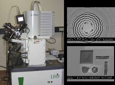
Key features of this microscope are the in-column secondary electron detector that provides low-noise imaging during FIB material removal as well as imaging at very low voltages.The unique objective lens design uses an electrostatic field below the lens (unlike competing design which utilizes a strong magnetic field, causing limitations in overall performance.
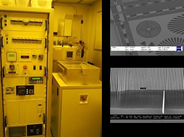
Dry Etching
|
|
STS MESC MULTIPLEX ICP, a manual wafer lock, high frequency ICP (Inductively Coupled Plasma) etch system for deep Si etching of up to 6-inch substrates. The plasma is inductively coupled at 13.56 MHz via a matching unit and coil assembly. Independent energy control is provided by biasing of the electrode (platen) via automatic power control and impedance matching. Several BOSCH like processes (alternating cycles of etching and surface passivation) have been implemented allowing high aspect ratio structures. Continuous mode for nanostructure fabrication is also available, down to the 10-nm scale in lateral resolution and aspect ratios of up to 10. The gases configured with this system include SF6 (Sulfur Hexafluoride), C4F8 (Octofluorocyclobutane), O2 (Oxygen), and Ar (Argon)
|
A 50 m2 class 1000 CR hosts the deposition equipments for thin films growth and surface functionalisation. In detail:
- Balzer metal evaporator, providing the possibility of 6 independent metal and semiconductors sources (4 e-gun based, 2 thermal);
- Magnetron Sputtering, for metals and ceramic materials deposition. Three independent targets can be used. The gases configured with this system are Ar, O2 and mix of Ar and O2, suitable for reactive deposition method of semiconductors and ceramics (SiO2, Al2O2, ITO). It is also possible to perform O2 plasma or Ar milling treatment on the sample for cleaning and surface activation prior to the deposition of sputtered materials.
- Chemical hood for wet etching processes, such as KOH anisotropic etching of silicon, Si isotropic etching, SiO2 HF based wet etching, metals wet etching for pattern transfer or dry etching metal mask production;
- 2 hoods for electrochemical growth of metals (Au, Cr, Ni, Cu) used for X-rays lithography mask or NIL moulds fabrication;
- CO2 Critical Point Drier.
In the CR is also available a Nitrogen filled Glove Box for O2 and water free processes such as Silanes functionalisation for mould antiadhesive coating or hydrophobic treatment. Moreover the GB is equipped with spin coater and controlled hot plate for the processing of moisture or oxygen sensible materials such as organic or hybrid semiconductors for PV cells or OLED. An evaporator is directly connected to the GB in order to avoid the contamination or the exposure to the air of the samples. The evaporator is equipped with three independent crucible for thermal metal evaporation and six sources for the growth of organic small molecules, fullerenes, LIF… The deposited materials films thickness is controlled in real time by a quartz balance.
Nanoimprint Lithograhy
Nanoimprint Lithography intensely investigated as the next manufacturing technology of present and future nanodevices. The nanoimprint technology would bring several benefits, such as low production costs, capability for extreme resolution (< 5 nm), in a highly controlled parallel patterning process over large areas.
The NIL Clean Room consists in 15 m² class 10 (ISO4) and 40 m² Class 1000 area. The laboratory hosts all the suitable equipments and tools in order to perform the NIL processes. In particular there are available:
- Spin coater in lamina flow class 10 hood for resist deposition;
- Hot plates with high temperature control (±1°C);
- A Paul-Otto Weber hydraulic press for standard thermal NIL processes;
- A UV NIL pneumatic press with possibility of 254 nm wavelength light exposure; it consist in a Hg vapor lamp that allows trough a suitable optical system the exposure of UV curable resist trough a quartz plate. The press has finely controlled hot plate in order to heat the sample during the imprinting procedure combining thermal and UV NIL processes;
- A chemical hood for simple wet processes (RCA cleaning, develop, metal etching);
- Optical microscope.
Moreover, the CR is equipped with the tools for SAM deposition for surface treatments. Surface functionalisation of moulds and stamps is basic step for NIL and UV-NIL techniques. For that purpose the laboratory is equipped with:
- A system for vapor phase deposition of silanes;
- Elipsometer for thin film thickness evaluation;
- Contact angle measure setup for evaluation of surface energy after surface treatments.
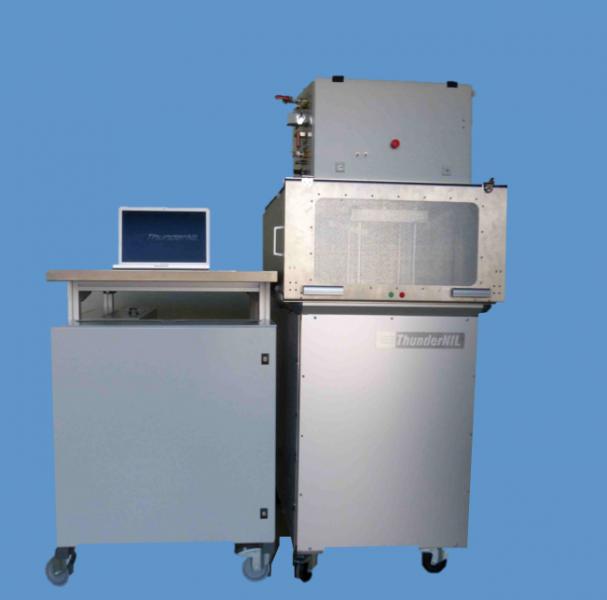 |
One of the main results of this research is the proprietary technology of "Pulsed-NIL" an ultrafast NIL process capable of nanostructuring full wafers in time scale of 100 microseconds.
The research activity has led to the foundation of a spin-off company, ThunderNIL (www.thundernil.com), with the purpose to transfer this new technology in production.
|