Labs And Facilities
Facilities
Beamline Stations at Elettra Synchrotron Storage Ring:
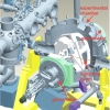
ALOISA
Developed for the study of surfaces and thin films, it can perform on in-situ grown samples several complementary techniques, such as X-ray Absorption and (Resonant) Photoemission Spectroscopies, X-ray photoelectron diffraction, Surface X-ray Diffraction, X-ray Reflectivity, Angle Resolved Electron Coincidence Spectroscopy
APE
Dedicated to the study of solid surfaces and nanostructured matter by means of several Spectroscopic techniques, such as ARPES, XAS, XMCD/LD, XPS, Mott magnetometry and also coupled with sophisticated off-line preparation/growth and characterization tools, such as atomically resolved STM, LEED-Auger, magneto-optical Kerr effect.
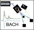
BACH
Multi spectroscopy beamline for the study of the electronic and magnetic properties of materials. In the 35 -1650 eV range fast HR-XPS, RESPES, energy-dependent ARPES and PhD, XMCD, XLD time resolved-XAS, XES and RIXS can be performed in the same chamber also on in-situ grown samples. ±6.5 T XMCD is also available
BEAR
Variable light polarization (linear, right/left elliptical polarization), wide photon energy range, high flexible scattering geometries. Photon-in-photon-out and photon-in-electron-emission processes for the study of materials, mainly ultra thin films and layered materials of basic science and technological interest.
GasPhase
Specifically devoted to research on isolated systems in the gas phase. Multi-technique approach for investigating electronic properties of free atoms, molecules and clusters: basic processes like inner-shell and multiple excitations and ionisation and key processes relevant to several areas of science and technology.
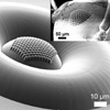
LILIT
LILIT (Laboratory for Interdisciplinary LIThography) beamline is devoted to the fabrication, by means of X-ray, e-beam and nanoimprint lithography, thin film deposition techniques and plasma etching, of structures of micro and nano resolution level, taking advantage of the high brilliance of Elettra
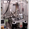
EndStation for X-ray Spectroscopy at ESRF:
LISA
Beamline for hard X-ray Absorption Spectroscopy (XAS). Wide energy range, high intensity and small sized beam. Energy-resolving X-ray detectors and measurement chambers for surface XAS. This beamline is particularly adapted for studies on trace elements, thin films, interfaces.
EndStations for Neutron Scattering techniques hosted at Institut Laue-Langevin
BRISP
Best-suited to the Neutron Brillouin Scattering technique to study the collective dynamics in a wide class of disordered systems (biological and aqueous systems; associate, quantum and metallic liquids; glasses; confined liquids…) as well as the spin dynamics at low momentum transfer in magnetic materials.
IN13
The thermal backscattering spectrometer IN13 at the Institute Laue-Langevin is mainly devoted to life sciences, in particular to the study of the dynamical features of macromolecular compounds in the µeV energy region, but scientific applications can be also found in areas of materials science, solid-state physics, geophysics and chemistry.
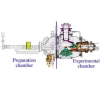
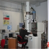
Equipment available @ TASC, Trieste:
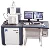
Scanning Electron Microscope
ZEISS SUPRA 40 high resolution Field Emission Gun (FEG) SEM with GEMINI column providing excellent imaging properties combined with analytical capabilities.The microscope is also equipped with a Energy Dispersive X-ray Spectrometer (EDS) EDAX for chemical characterisation.
EndStation at FERMI experimental hall:
SPRINT Laboratory
A new endstation for the generation of high harmonic at high repetition rate. It is addressed at the study of ultrafast magnetic processes in solid state physics by means of an upgraded vectorial Mott detector and a hemispherical electron analyser, suited to perform narrowband time-resolved valence band photoemission spectroscopy and spin detection.
Laboratories
Research Unit in Perugia: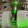
Brillouin Light Scattering for UHV studies
Growth of magnetic thin films in Ultra High Vacuum by means of e-beam evaporators, characterization with a LEED-Auger system and a Brillouin Light Spectroscopy apparatus
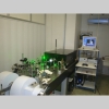
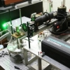
Conventional and µFocus BLS
Conventional BLS with wave vector resolution is used to measure the dispersion (frequency vs wave vector) of the spin waves of magnetic nanostructures in the dipole-exchange regime while micro-BLS is applied to map the spin wave intensity profile with spatial resolution of about 250 nm.
Photon Correlation Setup
A Goniometer with a special accommodation for samples can host aqueous solutions, molecular liquids, polymers and glues. The Photoncorrelation Spectroscopy (PCS) system can cover a dynamic range over ten decades (25ns-1310s).
Headquarters, Trieste TASC:

Analytical Laboratory
Growth in Ultra High Vacuum of thin films by means of Chemical Vapour Deposition (CVD) & Plasma Enhanced CVD (PECVD), characterization with Ultra-violet and X-ray photoemission spectroscopy (UPS and XPS), Auger electron spectroscopy, electron energy loss spectroscopy (EELS) and low energy electron diffraction (LEED).
SIPE Laboratory
Growth of thin films in Ultra High Vacuum, characterization by means of Auger Electron Spectroscopy (AES), Low Energy Electron Diffraction (LEED) and Inverse Photoemission, with Geiger Mueller detectors
Center for Electron Microscopy (CME)
TEM JEOL 2010 UHR FEG TEM/STEM with EDXS for elemental mapping and quantification; specimen preparation (grinders for mechanical thinning, two ion beam milling stations and plasma cleaner); commercial and home developed codes for digital processing and simulation of images and spectra
Variable and Low Temperature STMs
Variable Temperature (140K-900K) and Low Temperature (2.5K-300K) STMs. The VT system allows for imaging surface structure and dynamics, up to video-rate, also under exposure to reactive gas. The LT system can perform high resolution imaging of organic molecules as well as local electronic and vibrational spectroscopy.
Low Temperature STS-STM
Home made UHV scanning tunneling spectroscopy and microscopy system (STM and STS). Temperature range 5-300 K. Facilities for sample preparation and characterization in UHV, ion bombardment, low-energy electron diffraction, Auger spectroscopy.
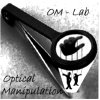
Optical Manipulation Laboratory
Optical manipulation by means of optical tweezers and laser microsurgery, pN force spectroscopy, TIRF and FRET microscopies applied to neurobiology, cancer cell biology, and nanobiotechnologies.

Bio-Nano-Sensors Laboratory
Nanoscience applied to biological and medical issues: nanoelectromechanical and plasmonic biosensors, DNA origami and biomechanical properties at the single cell and single molecule level.
NanoFabrication
Nano-lithography (E-beam, Ion Beam, Nanoimprint, X-ray, UV- and Soft Lithography) thin film deposition (thermal and e-gun evaporation, sputtering, electroplating), dry etching (RIE, RIE-ICP), for 2D and 3D micro- and nano-structuring, device fabrication (sensors, photovoltaic cells, microfluidic, optical and photonic devices…).
High Mobility Molecular Beam Epitaxy
The HMMBE laboratory is devoted to the epitaxial growth of high purity III-V semiconductor heterostructures for transport and photonic devices, and of site-controlled low-dimensional quantum nanostructures
Molecular Beam Epitaxy
Growth and characterisation of epitaxial layers and nanowires based on III-V and II-VI semiconductor compounds for electronic and optoelectronic applications.
Oxide Beam Epitaxy
Epitaxial growth of oxide heterostructures in UHV with precise atomic-layer control during interface construction using in situ RHEED (reflection high-energy electron diffraction). Samples can be transferred under UHV to APE beam line, and variable-temperature MOKE and HAXPES chambers.