A Roadmap for Controlled and Efficient n-type Doping of Self-assisted GaAs Nanowires Grown by Molecular Beam Epitaxy
N-type doping of GaAs nanowires has proven to be difficult because the amphoteric character of silicon impurities, routinely used for the n-type doping of GaAs epilayers, is enhanced by the nanowire growth mechanism and growth conditions. Among the various possible donor impurities for GaAs NWs, tellurium represents a good candidate since it is a very effective dopant in GaAs epilayers and does not present any risk of amphoteric behavior.
We demonstrated the growth of n-type GaAs nanowires by self-assisted molecular beam epitaxy using Te donors. Carrier density and electron mobility of highly doped nanowires were extracted through a combination of transport measurement and Kelvin probe force microscopy analysis in single-wire field-effect devices. Low-temperature photoluminescence was used to characterize the Te-doped nanowires over several orders of magnitude of the impurity concentration.
The ensemble of experiments demonstrated that Te, obtained from a GaTe source, can be reliably used to achieve free electron density as high as 1020 electron/cm3 in GaAs NWs grown by self-assisted MBE. An effective incorporation of Te can be obtained in NWs also at growth temperatures considerably higher than those used for Te doping in 2D MBE, as long as a significant flux of Te atoms, is provided. This feature allows the optimization of the NW morphology, as well as reducing the presence of unwanted impurities, while maintaining a high carrier density. The n-type NWs obtaind by this work, being produced without the use of gold nanoparticles to induce one-dimensional growth, are candidate to be integrated in the Si technology platform.
 |
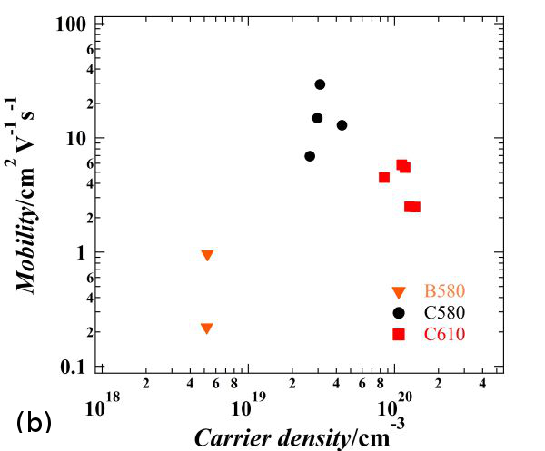 |
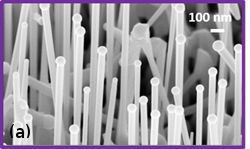
| (a) SEM image of Te-doped GaAs nanowires grown at 610° C with a Te flux corresponding to a carrier density n = 1 1019 cm-3 in MBE grown epitaxial layers | (b) carrier density and mobility values evaluated by transport measurements on single-nanowire field-effect devices at room temperature. The sample imaged in (a) is C610. |
Publication and authors:
Marta Orrù, Eva Repiso, Stefania Carapezzi, Alex Henning, Stefano Roddaro, Alfonso Franciosi, Yossi Rosenwaks, Anna Cavallini, Faustino Martelli, and Silvia Rubini
Adv. Funct. Mater. 2016, DOI: 10.1002/adfm.201504853