
Surfaces, films and interfaces
Surfaces, films and interfaces
|
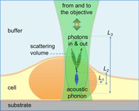
A multitude of fundamental chemical and physical processes occurs at surfaces and interfaces that drives the behavior of catalysts, chemical sensors, and devices for optoelectronics, light harvesting/conversion, magnetic applications. Thin films of the order of a few nanometers in thickness have been shown to be useful analogues of bulk materials. At the same time, tailoring the film size at the nanoscale allows the fine tuning of the electronic properties due to the quantum confinement. The study of surfaces and thin films has driven the development of a number of technologically advanced experimental techniques in order to probe and modify such systems down to the scale of single atoms. For example, the surface reactivity and conductivity of many transition metal oxides, TMO, is much relevant for the fabrication of efficient catalysts and photovoltaic cells (e.g. TiO2). The electronic properties of TMOs depend on the possibility of locally inject charge, which is made available elsewhere by the surface for triggering chemical reaction or for being extracted. |
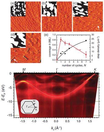
Scanning tunneling microscopy characterization of the graphene growth in Ir(111) and ARPES map showing the dispersion of the π band for the ΓK and ΓM directions M. Kralj et al. Physical Review B, 84, 075427 (2011) - Data collected at APE beamline, Elettra. |
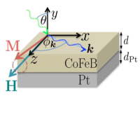
The atomic distribution of the charge in the surface and nearby layers can be probed by means of resonant photoemission, which allows one to achieve chemical sensitivity in the valence band. In particular, one can discriminate among atoms of the same species but with different ionization states. The corresponding intensity enhancement of the photoelectron yield can be valuably exploited also to study the distribution of dopants in highly diluted semiconductors (e.g. MnxCd1-xTe). The magnetic ordering and coupling in diluted magnetic systems (e.g Fe/(Ga,Mn)As) or in ferromagnetic metal/semiconductors heterojunctions (e.g. Mn/Si, Mn/Ge) are very suitable to realize structures in which the magnetic properties of the semiconductors are controlled by designed magnetic ions or to combine silicon technology with the functionality of magnetic systems, making these systems promising for applications in the field of spintronics. The ferromagnetic ordering of these systems can be revealed by x-ray circular magnetic dichroism measurements, probing the magnetic properties of specific elements in thin films that cannot be explored with conventional magnetic tools due to the reduced layer thickness. The combination of scanning tunneling microscopy and high resolution angle resolved photoemission spectroscopy reveal the growth morphology and the peculiar electronic properties of graphene/metal interfaces (e.g. graphene/Ru, Ir, Pt) and the chemically modified (doped or functionalized) graphene or graphene oxide layers by self-assembling of on-purpose synthesized organic precursors with tailored features.