Semiconductor Nanowires Growth
Semiconductor Nanowires Growth
Contact persons: Silvia Rubini, Alfonso Franciosi, Valentina Zannier
|
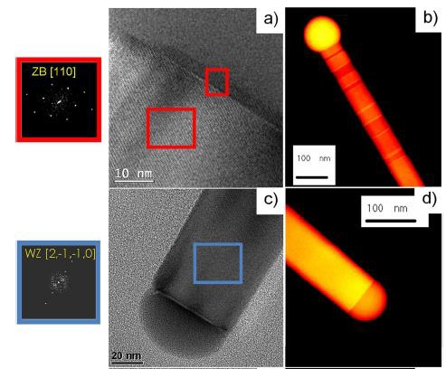
Semiconductor nanowires are ideally 1-D nanostructures with diameter in the 1-100 nm range and in principle unconstrained length. These systems are attracting increasing interest for the possibility they offer to exploit the properties related to their nano-scale size and their high surface to volume ratio in novel devices for electronics and optoelectronics. NWs can be obtained by different growth methods and the anisotropic growth is typically induced by the presence of a metal nanoparticle that is found at the NW tip at the end of the process. The activity of the molecular beam epitaxy (MBE) group is devoted both to the study of the growth mechanism of III-V (GaAs, InAs, InGaAs) and II-VI (ZnSe, CdSe) nanowires by MBE assisted by metal nanoparticles and to the investigation of the nanowire properties. Concerning the characterisation of the NWs, we investigated their morphological, structural, optical and electronic properties, via scanning and transmission electron microscopy, photoluminescence spectroscopy, optical reflectivity and spatially resolved syncrotron radiation photoemission spectroscopy, in by house activity and thanks to collaborations with CNR Institutes (IMM, IMEM, Nano) and ELETTRA Synchrotron radiation center |
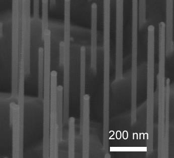
Top: as grown GaAs nanowires grown by Au-assisted MBE |